Logic gate
A device that is use to implement the Boolean function is known as logic gate.
A computer carries out all operation by mean of combinations of signal passing through standard block of built-in circuit known as logic gate. A logic gate is an electronic device that is use to operate one or more input signal to produce standard output signal.
In a computer when we build an electronic device we combine a multiple logic gates of different types. There are many types of logic gates are available but we can discuss some of the most important ones.
#AND gate
#OR gate
#NOT gate
#NAND gate
#NOR gate
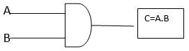
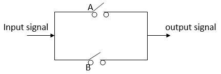
AND gate
An AND logic gate is created on the basis of multiplication operation. AND logic gate is electronic device that generate an output signal of 1 only if all input signal are also 1.
Example:
we connected two or more switches in series that behave as AND gate. The input current will reach the output point only when both the switch is in ON state. There will be no output if either one or both switch in OFF state.
![]()
Truth table of AND gate
The state of output signal depended on the combination of input signal.
| Inputs | Outputs | |
| A | B | C=A.B |
| 0 | 0 | 0 |
| 0 | 1 | 0 |
| 1 | 0 | 0 |
| 1 | 1 | 1 |
Block diagram of logic gate
OR gate
An OR logic gate is created on the basis of addition operation. OR logic gate is electronic device that generate an output signal of 1 if any of input signal are also 1.
Example:
we connected two or more switches in parallel that behave as OR gate. The input current will reach the output point when any one or both the switch is in ON state. There will be no output only when the switch in OFF state.
Truth table of OR gate
The state of output signal depended on the combination of input signal.
| Inputs | Outputs | |
| A | B | C=A+B |
| 0 | 0 | 0 |
| 0 | 1 | 1 |
| 1 | 0 | 1 |
| 1 | 1 | 1 |
Block diagram of OR gate

NOT gate
An NOT logic gate is created on the basis of complementation operation. NOT logic gate is electronic device that generate reverse of the input signal as output signal. This is also known as inverter because it inverts the signal.
The complementation operation is the unary operation that is defines on a single variable. NOT gate have always single value or signal input.
Truth table of NOT gate
| Input | Output |
| A | Ā |
| 0 | 1 |
| 1 | 0 |
Block diagram of NOT gate

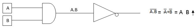
NAND gate
The NAND gate is the complemented of AND gate. The output of NAND gate is 1 if any one of the inputs is 0 and it will be 0 only when all input are 1.
Truth table of NAND gate
The state of output signal depended on the combination of input signal
| Inputs | Outputs | |
| A | B | C= |
| 0 | 0 | 1 |
| 0 | 1 | 1 |
| 1 | 0 | 1 |
| 1 | 1 | 0 |
Block diagram of NAND gate
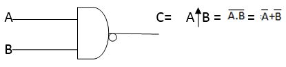
An AND gate followed by a NOT gate operates as a NAND gate. Output of the NAND gate is A.B that is fed as input to the NOT gate finally output is complement of A.B which is equal to (![]() ) or
) or ![]() or A↑B.
or A↑B.
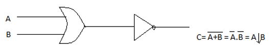
NOR gate
NOR gate is the complemented of OR gate. Output of NOR gate will be 1 only when all input are 0, and it will be 0 if any input as a 1.
Truth table of NOR gate:
| Inputs | Outputs | |
| A | B | C= |
| 0 | 0 | 1 |
| 0 | 1 | 0 |
| 1 | 0 | 0 |
| 1 | 1 | 0 |
Block diagram of NOR gate
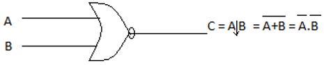
An OR gate followed by a NOT gate operation as a NOR gate. Output of the OR gate is A+B that in turn is fed as input as input to NOT gate finally output is complement of A+B which is equal to ![]() or
or![]() or A↓B.
or A↓B.